In the last years, the research on quantum technologies has grown dramatically targeting the development of novel computer architectures outclassing the current binary calculators. However, the complexity of these new devices puts severe constraints on the material quality and fabrication methods, so that acquiring control on their structure and morphology down to the scale of few nanometers becomes fundamental. The exploitation of innovative materials and the development of advanced growth methods are then crucial for the success of this research field.
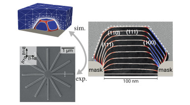
A study developed thanks to the collaboration between the experimental group of prof. Erik Bakkers of the Eindhoven University of Technology and the modelling team of Roberto Bergamaschini, Francesco Montalenti and Leo Miglio of the Department of Materials Science of the University of Milano-Bicocca, and recently published on the prestigious journal Advanced Functional Materials (Impact factor: 19, Journal Citation Reports (Clarivate Analytics, 2023)) with the title “"In-Plane Nanowire Growth of Topological Crystalline Insulator Pb1−xSnxTe” (doi: 10.1002/adfm.202305542), reveals the possibility of growing PbSnTe nanowires of very high quality, having the property of topological crystalline insulator ideal for the development of quantum devices. This achievement has been possible by exploiting advanced methods of selective deposition, optimized through the synergistic use of crystal growth simulations, performed by a phase-field code developed by the Milano-Bicocca’s group itself, and high-resolution electron microscopy analysis, in such a way to control the nanowire faceting, responsible for the topological properties. The assessment of the key thermodynamic and kinetic factors driving the morphological evolution reported in this study paves the way for the future application of PbSnTe in the more complex geometries of interconnected networks required for the fabrication of proper Qubits.