Organic molecular films and heterostructures
Thin films of organic molecular materials are grown and studied for possible applications as materials for light harvesting, energy and charge transfer, energy management, and as semiconducting materials in devices. To reach a high control over the film properties, growth is carried out via organic molecular beam epitaxy (OMBE) by tuning the conditions, such as pressure, substrate type and temperature, deposition rate, controlled storage after growth. The main interest of the group rests in the intrinsic properties of the molecular materials in the solid state, in particular in the form of thin layers or heterostructures of controlled crystalline quality. In addition, physical phenomena such as energy and charge transfer, singlet fission and triplet fusion, which are of possible interest for applications, are studied. The physics of such phenomena is characteristic of molecular materials and is closely linked to intermolecular interactions and thus to the structure of the material in the solid state. In the last years, several molecules have been considered, for example several oligothiophenes, oligocenes, and porphyrins.
The study of the OMBE process itself is carried out by analysing in-situ and in real time the properties of the growing samples, but also by monitoring in time the properties of the samples after the growth. The morphology and structural properties of the samples, closely related to the growth conditions, are studied ex-situ, mainly by atomic force microscopy; in addition, the optical properties of the molecular films are studied ex-situ in comparison with the single crystal properties, again as a function of the growth conditions. Thorough well-established collaborations, the structure of the thin films is checked by X-ray diffraction and, for some materials, in-situ PL and transient PL, are studied.
The growth of films of different molecules on high quality single crystal substrates, made of the same or similar molecular organic compounds, enables the study of the conditions for epitaxy, therefore the fabrication of heterostructures with high quality interfaces and controlled properties. Finally, with a view to device applications and for further characterization, different techniques for transferring the thin films from the original substrates to other, more suitable substrates are applied, while retaining the overall material properties.
Research Group
Prof. Adele Sassella
Dr. Alessandro Minotto
Research Lab
OMBE Lab – U5 Building, Ground Floor, Rooms T044A/B – T072
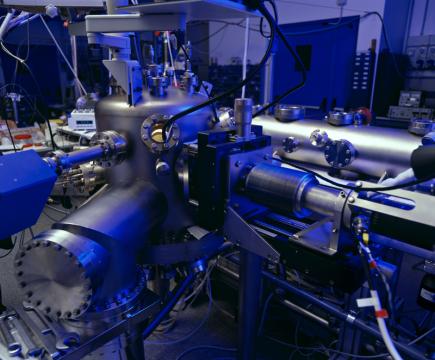
Facilities

The OMBE apparatus consists of high vacuum and ultra-high vacuum chambers where up to six sources can be installed for depositing different compounds; during OMBE growth, the film thickness is monitored in situ by a quartz microbalance. Optical spectroscopies, such as absorption, reflection, photoluminescence (PL) and ellipsometry, are used for the study of thin films and multilayers; PL is also applied in-situ to monitor the growth. Optical measurements can be carried out as a function of temperature, down to few K, under polarized light and at different incidence angles. Atomic force microscopy is used ex situ for the morphology characterization of all the samples and for the study of the film growth process; morphology is usually checked over several μm2 wide regions, while on crystalline samples molecular resolution is also achievable.