Characterization of materials electronic structure through X-ray photoelectron spectroscopies
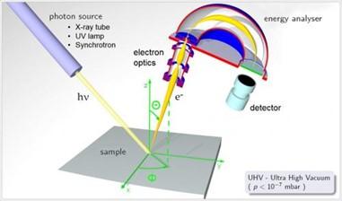
Our research activities are focussed on the characterization of materials through photoelectron spectroscopy techniques. In these experiments we collect and analyse the electrons emitted by the sample due to the photoelectric effect upon exposure to various monochromatic light sources. The photon energies suitable to photoemission ranges from hard x-rays to UV, allowing for the extraction of different physical and chemical properties. All experiments are carried out in ultra-high-vacuum conditions (UHV), ensuring a perfect isolation of specimen surfaces from external contaminations.
X-ray photoelectron spectroscopy
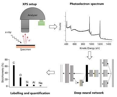
The application of x-rays to photoelectron spectroscopy (XPS) allows for the identification of atomic species and their chemical bonding type. XPS can be applied to any UHV compliant sample and thus it is a fundamental tool for research, especially where the materials surfaces and interfaces are relevant. For example, XPS has been applied to semiconductors, oxides, solar cells, gas sensing materials, functionalized surfaces and many more. XPS analysis can be also extended to other properties, such as local crystal structure, depth profiling analysis, interface junction energy diagrams or evaluation of charge-transfer state of complex materials. We are also investigating the possibility to speed up and improve the XPS spectra analysis through machine learning techniques.
Ultraviolet and angle-resolved photoelectron spectroscopy
UV based electron spectroscopy (UPS) gives a better insight about the sample valence band, i.e. about the energy region where the actual chemical bond takes place. This technique can be applied to any conductive material, both crystalline or polycrystalline, or to characterize the properties of surface adsorbed molecules.
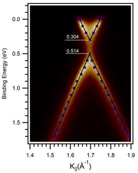
Furthermore, when carried out with a modern angle-resolved analyser (ARPES, angle-resolved photoelectron spectroscopy), this technique allows for the direct measurement of crystalline materials band structure. ARPES is then the best tool for the exploration of several interesting materials which display quantum properties, such as 2D compound (e.g., graphene), topological insulators and high temperature superconductors.
Photoelectron spectroscopy lab
We are in the design stage of the future XPS-ARPES lab. The main goal is to provide an high performance tool, compatible with most of the department research topics, with free customization and expandability options. The system will include:
- A high resolution, angle resolved electron analyser, fully compatible with XPS and UPS/ARPES;
- A mechanized five axis manipulator, with cryocooling;
- Multiple X-ray and uv sources, both mono and non-monochromatic;
- Tools for sample cleaning and for insulating sample analysis;
- A fast entry coupled with a glove-box, in order to evaluate oxygen-sensitive samples;
- Expandability for additional UHV chambers for in-situ growth and manipulation.
We will also consider to expand towards additional facilities, such as near-ambient pressure XPS (NAXPS) and hard x-rays photoelectron spectroscopy (HAXPES).
Principal Investigator
Prof. Giovanni Drera