Transition Metal Dichalcogenides (TMDs) are a versatile class of materials with immense potential for fields of application, from nanoelectronics and optics to sensing and catalysis. TMDs are inherently imperfect, containing defects such as vacancies and boundaries that significantly impact on their properties. Defects are often considered detrimental due to their negative effects on some materials’ properties like mechanical and chemical stability, or alterations in electrical transport. However, they can also offer unique beneficial effects, enhancing and/or introducing functionalities in materials. For instance, sulphur atomic vacancies (VS) in MoS2 are predicted to boost thermoelectric and electrocatalytic performance, even though the loss of electrical conductivity caused by an excess of defects could limit its experimental efficiency. To this purpose, defects engineering is the pivotal approach for optimizing defective materials for specific applications. Electrochemical nanopatterning is a promising technique to precisely control the distribution of defects within a material and consists in creating spatially defined regions with chemically active defects interconnected by pristine material areas, preserving the original materials’ properties. Pristine zones ensure efficient electrical connection between the defective but active zones through the pristine material zones, bypassing the adverse effects of defects on electrical conductivity. In addition to this, patterning allows for functional properties tuning, by finely controlling the local defect density in the treated zones.
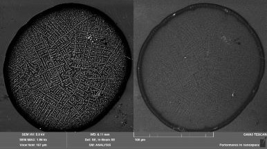
In this work, we employed Electrochemical nanoLithography (EnL) to create and precisely control high-density sulphur atomic vacancies on the surface of a MoS2 thin film. I this way, it has been possible to tune the electronic properties and to generate the corresponding functionalities in a controlled manner. To evaluate the effects of patterning, we investigated its effectiveness in electrocatalytically promoting the Hydrogen Evolution Reaction (HER), an application of fundamental importance for which MoS2 is considered as a potentially highly efficient non-precious electrocatalyst. The results demonstrate that EnL enables spatial control with remarkable resolution in the submicrometric range confined to the surface. Confocal μ-Raman spectroscopy, KPFM, μDR, and X-PEEM measurements confirm the formation of atomic vacancies only in the desired zones, generating unoccupied midgap states. Furthermore, we assessed through the HER that the spatial distribution of VS-rich printed zones enhances the electrocatalytic activity MoS2, with an improvement of more than five times compared to untreated material.
This work has been successfully carried out through a collaboration between a team of researchers of the University of Milano-Bicocca (S. A. Mirshokraee, G. Tseberlidis, M. Acciarri, C. Santoro) together with Istituto per lo Studio dei Materiali Nanostrutturati (CNR-ISMN; D. Gentili, E. Lunedei, F. Borgatti, A. Mezzi, G. Ruani, M. Cavallini), Istituto per la microelettronica e microsistemi (CNR-IMM; G. Calabrese, F. Liscio), Istituto per la Sintesi Organica e la Fotoreattivita (CNR-ISOF; V. Benekou, A. Candini, V. Palermo), Istituto di chimica dei composti organo metallici (CNR-ICCOM; E. Berretti, A. Lavacchi), Diamond Light Source (Harwell Science and Innovation Campus, Didcot, UK; F. Maccherozzi).
The results of the study are reported in the paper “Tuning Electronic and Functional Properties in Defected MoS2 Films by Surface Patterning of Sulphur Atomic Vacancies" (DOI: 10.1002/smtd.202401486) published on Small Methods (Impact Factor 10.7 - Clarivate 2023)